The Basics of Printed Circuit Board (PCB) Design

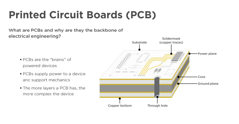
Printed circuit boards (PCB’s) have long been the foundation of electrical engineering, serving as the "brains" of any powered device. Designing PCB’s is to electrical engineering as HTML is to web development—the backbone that makes it all possible. That’s because no powered device works without a PCB of some sort. From cell phones and remote controls to robotics and toys, PCB’s provide electricity and connectivity between the components of a device, allowing it to function the way it was designed.
Here’s a look at what goes into this technology and what you need to know to get started prototyping a PCB for your next embedded system project.
PCBs on the Rise: Powering the Connected Devices
PCB Design has been around for decades, but its relevance is back in the spotlight. They originally came about to answer the need for smaller, more efficient ways to power electronics. In the age of the Internet where everyday devices with embedded systems are becoming Internet-connected devices, PCB design is still meeting that need, while growing more advanced, and more in demand.
The internet has brought us the ability to control everyday objects and devices remotely, from our phones. All of a sudden, household objects are mini-computers, able to be turned on through a mobile app. Wearables track our steps, and smart thermostats track our environments. Cars can monitor themselves, and bridges can sense structural failure. All of this requires hardware, software, and power.
For many of these devices to be "smart," they need to have PCB’s. So what are PCB’s exactly, and how are they made? Let’s break down the basics.
What Is a Printed Circuit Board?

Printed circuit boards are physical components of electronic devices. They’re made up of a board, which is typically resin or plastic, and solder, the conductive metal parts that channel energy, usually made of copper. The solder makes the electrical connections between the PCB and the parts of the device possible. There’s also a silkscreen layer on top of the board that indicates what goes where, like a roadmap.
PCB’s don’t just supply power; they also support the mechanics of a device. That’s because they not only route power, they route signals to different components. This is why a PCB acts like the brain of a device—and a device can’t function without it.
A PCB board is usually talked about in terms of how many layers it has, which can be anywhere from one to 10 layers. The more complex a device is the more layers the PCB will have. They can also be single- or double-sided, with copper layers on both sides. The more copper there is for connecting components, the more components you can have–hence, the more complex the device.
To get a PCB designed and manufactured, there are a few steps: schematic design, board design with EDA software, manufacturing, assembly, and testing.
DESIGNING, PRINTING, AND MANUFACTURING A PCB
A PCB design expert can assist you in assembling a top-quality PCB catered to your specific technological needs. A PCB designer will provide an in-depth analysis of your device’s requirements to ensure your product has the support necessary to excel in the competitive tech market. They’ll have access to all of the latest software and are well-versed in the best design strategies.
Once you have a PCB designer and you’ve gotten them up to speed on your project requirements, there are a few steps they’ll go through. Here’s a quick overview of the process.
1. The schematic for the circuit is designed.
First, a designer will create the schematic. A schematic is a crucial step before designing the board itself and should never be overlooked. A schematic is like a roadmap for a circuit, containing a series of symbols that represent aspects of the circuit: switches, resistors, diodes, nodes, and more. This is also helpful later on for troubleshooting any issues with your PCB.
2. Using EDA (or, ECAD) software, the board design is laid out.
After the circuit design is captured in a schematic, it’s translated into an electronic design automation (EDA) software packages. The design has to be exported into an industry standard format (e.g., the Gerber format, the default "language" used to describe PCB components). The resulting file acts as a set of instructions for the production phase of a PCB.
3. The PCB is printed, fabricated, and assembled.
Once you have a Gerber or CAD file, you can manufacture your PCB. The dimensions of the PCB—along with how many layers it will be—are decided, and all of the components are positioned, ground, and laid out, and signal traces dictated by the Gerber file. There are different requirements for different boards, so your PCB designer will be able to tell you whether you need surface mount (SMT), thru-hole, single- or double-sided fabrication, and more.
4. Test a PCB for functionality.
Finally, white-box testing will make sure your PCB is structured properly once it’s been fabricated. The goal here is to test every possible output to ensure the PCB is functioning as the designer intended it to. Compared with black box testing, which only tests inputs and outputs without looking at the specifics, white box testing focuses on the each possible pathway of the PCB to make sure there are no failures.

