Why Choose Fineline Circuits & Technology for PCB Fabrication Service?
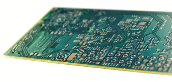
Fineline Circuits & Technology manufactures advanced PCB fabrication with consistent high quality and affordable pricing. Whether it is for prototype or large volume production runs, We can meet your PCB fabrication needs in a variety of materials and technologies. We focus on multi-layer, impedance controlled, and HDI PCB’s in varying complexities.
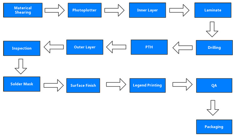
Our PCB Fabrication Process

Circuit Board Specifications
- Maximum Panel size: 24″ x 36″
- Maximum Number of Layers: 36
- Copper Thickness: 0.025oz to 20oz
- Minimum Line Width: 3mils
- Minimum Line spacing: 3mils
- Smallest Hole: 0.006″
- Micro & Laser Via
- Blind, Buried and plugged Vias
- Controlled impedance
- Depth Control/Cavity/Laser drilling
Material
- Thickness: 0.008″ to 0.500″
- High TG FR-4
- Polyimide
- PTFE, Duriod
- Aluminum Base
- Rogers
- Flex Laminate
- Embedded Resistors
- Or Any specialized material per your request
Solder Mask
- LPI – Green, Yellow, Black, Red, Blue etc.
- Peelable Mask
- Via Fill
- Copper fill
- Final Finishes
Surface Finish
- Carbon
- Selective Gold Plating
- Hard and Soft Gold
- Immersion Gold & Tin
- Immersion Silver & Palladium
- OSP
- Lead Free & Leaded Solder
Legend
- White
- Other colors per your request
Testing
- Electrical testing – Flying probe or Bed of Nails
- Sample lot inspection
- Cross-sectioning
Quality
- AOI
- 100% Visual inspection
Delivery
- Quick turn 24 to 48 Hours
- Standard Prototype: 5 to 15 days
- Standard Production: 10 to 20 days

